
DARLINGTON AMPLIFIER


INTRODUCTION TO DARLINGTON PAIR


In practice, the two transistors are put inside a single package and three terminals E, B and C are brought out as shown in figure.

darlington pair circuit


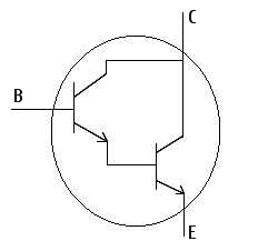
This three terminal device is known as darlington pair. It acts like a single transistor that has high current gain and high input impedence.


DARLINGTON AMPLIFIER

Darlington amplifier with voltage divider bias is shown in figure.


darlington amplifier circuit


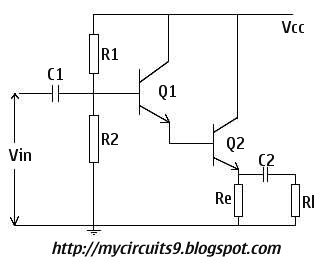
In this circuit the output of one amplifier is coupled into the input of the next one by directly joining emitter of one transistor to the base of Other. Obviously, the emitter current of the first transistor becames the base current for the second transistor.
The biasing analysis is similar to that of RC coupled Amplifier except that two Vbe drops are to be considered.


ADVANTAGES OF DARLINGTON AMPLIFIER
  • It uses very few components and can be readily formed from two adjacent transistors in an IC.

  • It provides excellent Characteristics of high input impedence with low output impedence and high current gain, all desirable Characteristics for a current gain amplifier.
APPLICATIONS OF DARLINGTON AMPLIFIER
It has enormous impedence transformation capability. Hence it is used as high gain operational amplifier which depends on very high input impedence for its operation as an integrator or summing amplifier in analogue applications.

SOME DARLINGTON PAIR CIRCUITS

Water Tank Overflow alarm circuit

Rain Detector and Alarm Circuit


Comments

Popular posts from this blog

Digital Fan Regulator Circuit Diagram

This is the project of Digital Fan Regulator Circuit diagram. The circuit presented here can be used to control the speed of  fans using induction motor. The speed control is nonlinear, i.e. in steps. The current step number is displayed on a 7-segment display. Speed can be varied over a wide range because the circuit can alter the voltage applied to the fan motor from 130V to 230V RMS in a maximum of seven steps.  The triac used in the final stage is fired at different angles to get different voltage outputs by applying short-dura-tion current pulses at its gate. For this pur-pose a UJT relax-ation oscillator is used that outputs sawtooth waveform. This waveform is coupled to the gate of the triac through an optocoupler (MOC3011) that has a triac driver output stage.  Pedestal voltage control is used for varying the firing angle of the triac. The power supply for the relaxation oscillator is derived from the rectified mains via 10-kilo-ohm, 10W series dropping/limit-ing...

Using the SG3525 PWM Controller Explanation and Example Circuit Diagram Schematic of Push Pull Converter

PWM is used in all sorts of power control and converter circuits. Some common examples include motor control, DC-DC converters, DC-AC inverters and lamp dimmers. There are numerous PWM controllers available that make the use and application of PWM quite easy. One of the most popular of such controllers is the versatile and ubiquitous SG3525 produced by multiple manufacturers – ST Microelectronics, Fairchild Semiconductors, On Semiconductors, to name a few. SG3525 is used extensively in DC-DC converters, DC-AC inverters, home UPS systems, solar inverters, power supplies, battery chargers and numerous other applications. With proper understanding, you can soon start using SG3525 yourself in such applications or any other application really that demands PWM control. Before going on to the description and application, let’s first take a look at the block diagram and the pin layout. Pins 1 (Inverting Input) and 2 (Non Inverting Input) are the inputs to the on-board error amplifier. If you a...

FM transmitter using UPC1651

Description. Here is the circuit diagram of an FM transmitter using the IC UPC1651. UPC1651 is a wide band UHF Silicon MMIC amplifier. The IC has a broad frequency response to 1200MHz and power gain up to 19dB.The IC can be operated from 5V DC. The audio signals picked by the microphone are fed to the input pin (pin2) of the IC via capacitor C1. C1 acts as a noise filter. The modulated FM signal will be available at the output pin (pin4) of the IC. Inductor L1 and capacitor C3 forms the necessary LC circuit for creating the oscillations. Frequency of the transmitter can be varied by adjusting the capacitor C3. Circuit diagram with Parts list. Notes. The circuit can be assembled on a Vero board. Inductor L1 can be made by making 5 turns of 26SWG enameled copper wire on a 4mm diameter plastic former. A ¾ meter insulated copper wire can be used as the antenna. Do not give more than 6V to the IC. Mic M1 can be a condenser microphone.